[2023-09-30]巴基斯坦防务论坛评论区:最新消息是,中国的7nm芯片采用同步辐射制造,其功率是EUV光刻的40倍。
文章原始标题:The latest news is that China's 7nm chips are manufactured using synchrotron radiation, which has 40 times the capacity of EUV lithography.
国外来源地址:https://pdf.defence.pk/threads/the-latest-news-is-that-chinas-7nm-chips-are-manufactured-using-synchrotron-radiation-which-has-40-times-the-capacity-of-euv-lithography.775756/
该译文由蓝林网编辑,转载请声明来源(蓝林网)
内容简介: 在国外盛传的中国“光刻厂”
MH.Yang
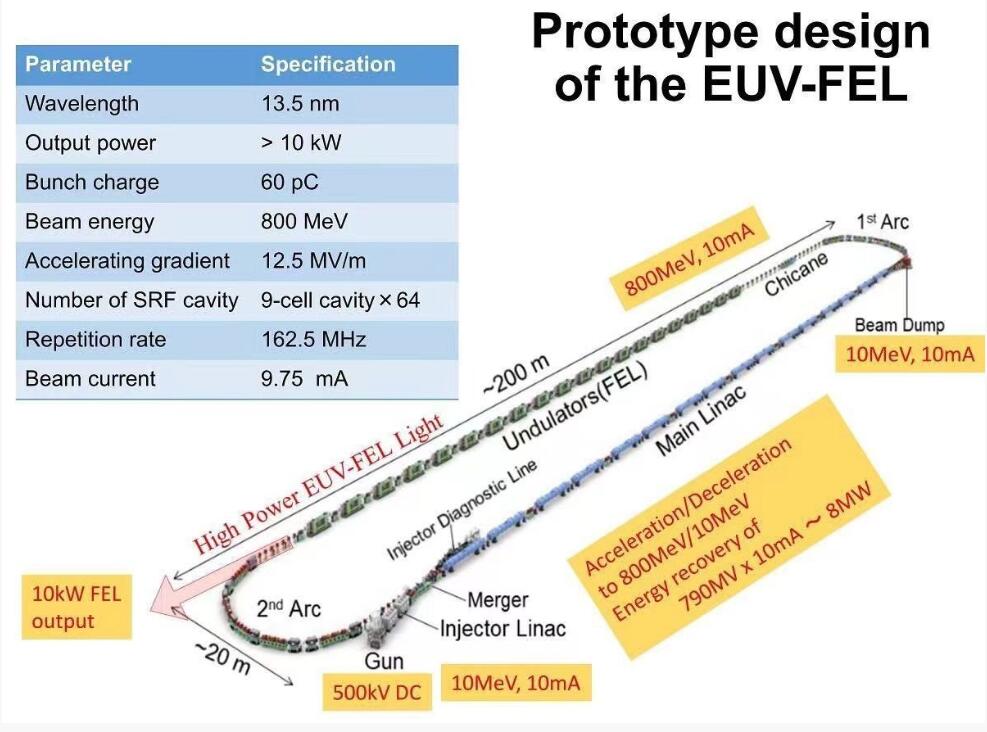
This large research facility was originally designed for scientific research in the extreme ultraviolet band.
这个大型研究设施最初是为极紫外波段的科学研究而设计的。
Bengal71 -> MH.Yang
Can you please provide some source of this news?
你能提供一些消息来源吗?
Menthol -> MH.Yang
So, it uses a different method.
No wonder Huawei dares enough to release his own chip.
I thought it used DUV tricks.
所以,它采用了不同的方法。
难怪华为敢于发布自己的芯片。
我还以为它是使用了某种DUV技巧。
White and Green with M/S -> MH.Yang
What is the source dude???
消息来源是什么???
Skull and Bones
That is a big innovation.
这是一项重大创新。
MH.Yang
Due to the global division of labour, if photolithography is too large to be transported from Europe to Asia, so the semiconductor industry is now using ASML's compact lithography technology.
The SSMB-EUV light source used in China has an output power of >100000KW, a capacity 40 times that of ASML, an accelerator length of >200 metres and a width of >20 metres alone, and it is capable of using dozens of EUVs at the same time with a beam splitter. The whole SSMB-EUV light source volume is equivalent to a photolithography factory. The construction of SSMB-EUV light source requires a complete industrial chain and huge capital investment, and China is the only country that can meet all the conditions.
由于全球分工,如果光刻机体积太大,就无法从欧洲运到亚洲,因此半导体行业现在使用的是 ASML 的紧凑型光刻技术。
中国使用的SSMB-EUV光源输出功率大于100000千瓦,功率是ASML的40倍,加速器长度大于200米,仅宽度就大于20米,通过分束器可以同时使用几十台EUV的能力。整个SSMB-EUV光源体积相当于一座光刻工厂。建设SSMB-EUV光源需要完整的产业链和巨大的资金投入,而中国是唯一能够满足所有条件的国家。
TriptiD
Source of this news ? What is the unit cost of chips manufactured using this technique?
新闻来源?使用这种技术制造芯片的单位成本是多少?
ziaulislam -> TriptiD
Cost...it's weird when talk about cost when it comes to China manufacturing thing
The question has been asked since 1990s and we deep down have always known the answer
Sooner or later China will get it done like it has always been the case
成本......当谈到中国制造的成本时,感觉很奇怪
这个问题自90年代就一直被问到,而我们内心深处始终都知道答案
中国迟早会像以往一样实现这项成就
TriptiD -> ziaulislam
We are not talking about t-shirts and towels here.
The reason that I am asking about costs is that the chips could have been made using new tech in an experimental setting- which could be prohibitively expensive in a commerical setting. For example, you can "manufacture " gold in a particle accelerator, but the cost is prohibitive.
我们不是在讨论T恤和毛巾。
我之所以要问成本问题,是因为这些芯片可能是在实验环境中,使用新技术制造的——在商业环境中,这种技术的成本可能高得令人望而却步。例如,你可以用粒子加速器“制造”黄金,但成本高得离谱。
ziaulislam -> TriptiD
No we are talking about solar panels and other electronics costs
Ultimately China will figure out how to decrease the cost
They always do
不,我们说的是太阳能电池板和其他电子产品的成本
中国最后都会想办法降低成本,他们总是这样做
epebble -> TriptiD
That question is easy to answer. If they sell only 100,000 7nm chips, your suspicion may be correct. But if they sell 100 million 7nm chips, they could not be making it at a loss and survive. In 2022, 1,400 million smartphones were sold. So, 100 million is only 7% of smartphones market.
这个问题很容易回答。如果他们只卖出10万片7纳米芯片,你的怀疑可能是正确的。但如果他们卖出了1亿个7纳米芯片,他们就不可能在亏损的情况下生存下来。2022 年,智能手机的销量为14亿部。所以,1亿只占智能手机市场的7%。
TriptiD -> epebble
Or they could just be using the existing process using ASML machines obtained by busting sanctions and not the technology the OP is claiming. That is why I asked him for the source of the news.
或者,他们可能只是通过打破制裁,使用获得的 ASML 机器的现有工艺,而不是题主所声称的技术。这就是我问他消息来源的原因。
epebble -> TriptiD
Unlikely. Even if they obtain them clandestinely, which is very difficult, as they are huge and enormously expensive and hence easily tracked. It is like surreptitiously buying a 747 or an aircraft carrier, they need huge amount of handholding services from the manufacturer. Imagine a large jet, times 1000. Can you steal this?
The $150 Million Machine Keeping Moore’s Law Alive
不太可能。即使他们秘密获得这些设备,也是非常困难的,因为这些武器体积庞大,价格昂贵,因此很容易被追踪到。这就好比偷偷购买一架 747 或一艘航空母舰,它们需要制造商提供大量的协助服务。想象一下,一架大型喷气式飞机,乘以 1000。你能偷到这个吗?
价值1.5亿美元的机器让摩尔定律得以延续
TriptiD -> epebble
You are forgetting even nations like Pakistan and North Korea have stolen missile and nuclear tech. So, yes, if China is motivated enough , they can definitely get an ASML machine by busting sanctions.
你忘了,就连巴基斯坦和朝鲜这样的国家也曾窃取导弹和核技术。所以,是的,如果中国有足够的动力,他们完全可以通过打破制裁获得 ASML 设备。
GreatHanWarrior -> TriptiD
Usually. Indians are better at these things. And they are proud of it.
通常情况下印度人更擅长这类事情。他们为此感到自豪。
epebble -> TriptiD
Missile and nuclear tech are easier than 7 nm. Neither Pakistan nor NK have high tech. Their roads, railroads and ports -19th Century technology - are built/supplied by China. Their challenge is to run a power grid.
导弹和核技术比7纳米更容易。巴基斯坦和朝鲜都没有高科技。他们的公路、铁路和港口都是19世纪的技术,都是由中国建造/提供的。他们面临的挑战是运行电网。
TriptiD -> epebble
The question was about STEALING, not about whether it is high tech or low tech. If I have enough money and not located in China, I can purchase a ASML machine, but I can't purchase missile or nuclear tech.
And if China has indigenously developed an alternate tech, why is it keeping so quiet about it ? Doesn't it want to boast to the world that it defeated US sanctions and get customers for its indigenous technology?
问题是关于“窃取”,而不是关于“高科技”或“低科技”。如果我有足够的钱,而且不在中国,我可以购买ASML设备,但我不能购买导弹或核技术。
如果中国已经自主研发了替代技术,为什么还要保持沉默?难道它不想向全世界夸耀自己战胜了美国的制裁,并为自己的本土技术争取客户吗?
BT -> TriptiD
None of these are true. Don’t water down China’s achievements in indigenizing semiconductor supply chain with fantasies.
这些都不是真的。不要用幻想来淡化中国在半导体供应链本土化方面取得的成就。
FS -> BT
It’s more BS from the US intelligence. They think that if they make ridiculous statements then no one will believe that China can make 7nm chips.
What the US government and bureaucrats don’t seem to understand is that no amount of BS and hot air can change what is really happening.
It doesn’t matter whether the Western population thinks that China can make 7nm chips or not. China is going to keep making them and build fabs to make them.
For some strange reason, they have replaced reality with propaganda and think that this will do something.
I’m still at a loss as to what they think will happen. No amount of propaganda helped the Nazis when they lost in WWII.
I read an article that the Germans were shocked when allied troops showed up outside Berlin and started hammering the city.
They thought they were winning WWII!
这更像是美国情报部门的胡说八道。他们认为,如果他们发表荒谬的言论,就不会有人相信中国能制造出7纳米芯片。
美国政府和官僚们似乎不明白的是,再多的胡说八道和空谈也无法改变正在发生的真实情况。
西方人是否认为中国能生产7纳米芯片并不重要。中国将继续生产7纳米芯片,并建立生产7纳米芯片的工厂。
出于某种奇怪的原因,他们用宣传取代了现实,并认为这样会有所作为。
我仍然不知道他们认为会发生什么。当纳粹在二战中失败时,再多的宣传也无济于事。
我读过一篇文章,说当盟军部队出现在柏林城外并开始轰炸这座城市时,德国人感到非常震惊。他们还以为自己赢得了二战!
etylo -> TriptiD
Chinese are not boastful like you Indians, don't think every one is like you.
中国人不像你们印度人那样爱吹牛,不要以为每个人都和你们一样。
GreatHanWarrior -> TriptiD
So. Please prove that the Chinese 7nm chip uses ASML EUV.
Please prove. Thank you.
那么请证明中国的7纳米芯片使用的是 ASML 的EUV光刻机。
请证明。谢谢。
beijingwalker -> TriptiD
Funny words from someone whose media produces the most lies in the world.
India has more fake news than any other country in the world
Nearly 60% of Indians had seen fake news against the global average of 57%, said a recent survey. Overall, India ranked seventh in Microsoft’s ‘Digital Civility’
来自一个媒体制造了世界上最多谎言的国家的人,说出一些滑稽的话
印度的假新闻比世界上任何国家都多
最近的一项调查显示,近 60% 的印度人看到过假新闻,而全球平均比例为 57%。总体而言,印度在微软的“数字文明”中排名第七。
TriptiD -> beijingwalker
I have said so many times that I can't prove it because I don't even know if its true.
I am sure Tsinghua is doing some cutting edge research in the field. I doubt that the tech used in the SMIC chips in the Huawei chips is fully Chinese, but if someone presents evidence to that effect, then I will admit my doubts were ill-founded.
My understanding is that until now the known processes for making those chips required ASML machines. I am not saying China has not developed an alternative, only that there is no public records or evidence about what that process is.
我说过很多次,我无法证明它,因为我甚至不知道这是不是真的。
我相信清华正在该领域开展一些前沿研究。我怀疑华为芯片中使用的中芯国际芯片技术是否完全是中国的,但如果有人提出这方面的证据,我会承认我的怀疑是没有根据的。
我的理解是,到目前为止,制造这些芯片的已知工艺需要 ASML 的设备。我并不是说中国没有开发出替代方案,只是没有关于这一过程的公开的记录或证据。
Menthol -> TriptiD
That is the news.
Because Huawei is able to produce 7nm chips without ASML.
And now everyone is investigating and proposing several theories about it.
Up to now, no one really knows the truth.
My theory is probably a DUV trick, as SMIC launched 7nm processor for bitcoin mining using a DUV trick last year.
And it's not a coincidence because Huawei is launching 7nm processor instead of 5nm or 3nm.
这就是新闻。
因为华为能够在没有 ASML 的情况下生产7纳米芯片。
现在,每个人都在对此进行调查并提出了一些理论。
到目前为止,没有人知道真相。
我的推测可能是某种 DUV 技巧,因为中芯国际去年推出的用于比特币挖矿的7纳米处理器就使用了一种DUV技巧。
这并非巧合,因为华为推出的是7纳米处理器,而不是5纳米或3纳米处理器。
GreatHanWarrior -> TriptiD
If India wants to look different from Pakistan. India develops its own technology first!
Currently, even cameras. India still relies on Chinese technology. India and Pakistan are not too different.
如果印度想看起来与巴基斯坦有所不同。印度要先发展自己的技术!
目前,即使是摄像头,印度仍然依赖中国技术。印度和巴基斯坦并没有太大区别。
GreatHanWarrior -> TriptiD
Let me talk about a common sense topic - if Huawei chips use ASML. Americans will know Mate 60 before Chinese people.
The fact is. The ASML owned by China cannot manufacture 7nm chips.
Huawei 7nm chip is completely based on Chinese semiconductor technology!
让我来说一个常识性的话题——如果华为芯片使用的是ASML设备。美国人会比中国人更早知道Mate 60的。
事实是,中国拥有的ASML设备无法生产7纳米芯片。
华为7纳米芯片完全基于中国的半导体技术!
MH.Yang
The news comes from a product launch on 12 September 2023 reported by Huawei. Huawei mentions that they work with the Beijing Synchrotron Radiation Facility, BSF, on chips. Then the Chinese media enquired about its two factories in Xiongan and Shanghai, owned by CGST and Zhangjiang Hi-Tech, that can manufacture 7nm chips via synchrotron radiation.
The Beijing Synchrotron Radiation Facility, BSF, and Tsinghua University have collaborated to propose the SSMB-EUV light source solution (Steady State Microbeam), which overturns the concept of traditional lithography technology by no longer relying on shrinking the light source to improve the quality of the image, but rather, by enlarging and elongating the light source, to achieve the automatic adjustment of the different wavelengths of light, so as to achieve a higher degree of precision.
Of course, all the news now comes from the unofficial media splicing bits and pieces together and making guesses. It has not been confirmed by official organisations such as Huawei or Tsinghua University. I can understand if people don't believe it.
Satellite view of SSMB-EUV light source factory:
In June 2021, the official Chinese government media reported on the completion of the construction of the SSMB-EUV light source factory:
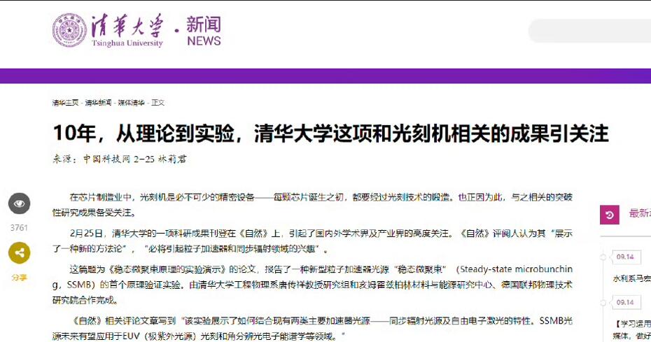
In February 2023, a press release from Tsinghua University's official media stated that the university's SSMB-EUV light source solution and technology had been put to practical use after spending 10 years and had solved a problem that was a major national need in the field of photolithography:
这一消息来自华为公司于2023年9月12日的产品发布会。华为提到,他们与北京同步辐射中心(BSF)合作开发芯片。随后,中国媒体询问了CGST 和张江高科在雄安和上海的两家工厂,这两家工厂可以通过同步辐射生产7纳米芯片。
北京同步辐射中心(BSF)与清华大学合作,提出了 SSMB-EUV 光源方案(稳态微聚束),颠覆了传统光刻技术的概念,不再依靠缩小光源来提高成像质量,而是通过放大和拉长光源,实现不同波长光的自动调节,从而达到更高的精度。
当然,现在所有的消息都来自非官方媒体的拼凑和猜测。华为或清华大学等官方机构并未证实此事。如果人们不相信,我可以理解。
SSMB-EUV 光源工厂卫星图:

2021 年 6 月,中国官方媒体报道了 SSMB-EUV 光源工厂竣工的消息:

2023 年 2 月,清华大学官方媒体发布新闻稿称,该校的 SSMB-EUV 光源方案和技术历经 10 年时间终于投入实际应用,解决了光刻领域的国家重大需求问题:
Menthol -> MH.Yang
I think this project is not related to the current Huawei 7nm chips.
I think this project is aiming for 1nm chips in the future.
There are still several years away for the launching of 1nm chips, there are still a lot of time for China.
I also wonder, what is China progress on the carbon or graphene based chip?
我觉得这个项目与目前的华为7纳米芯片无关。
我认为这个项目的目标是未来的1纳米芯片。
距离推出1纳米芯片还有几年时间,中国还有很多时间。
我还想知道,中国在碳基或石墨烯基芯片方面有什么进展?
FuturePAF -> Menthol
Or some kind of glass based chips?
Intel seems pretty excited about glass substrates
Intel has announced a a glass substrate breakthrough, which will make its future chips faster and more efficient.
或者某种玻璃基芯片?
英特尔似乎对玻璃基板非常感兴趣
英特尔公司宣布了一项玻璃基板突破,这将使其未来的芯片速度更快、效率更高。
TriptiD -> MH.Yang
Thanks for posting this. I have met a lot of really smart Tshingua graduates, so I have great respect for this university. However, the leap from research in a university and commerical production is a big one and your posts don't provide enough authoritative information to demonstrate this has been done. My main concern is what the unit cost of production will be, taking into account capital costs. The chips in the new phone carry the SMIC label. How is SMIC involved in the process you have described ?
谢谢你发布的这篇文章。我见过很多非常聪明的清华毕业生,因此我非常尊重这所大学。但是,从大学研究到商业化生产是一个巨大的飞跃,而你的帖子没有提供足够的权威信息来证明这一点。我主要关心的是,考虑到资本成本,单位生产成本会是多少。新手机中的芯片贴有中芯国际的标签。中芯国际是如何参与你所描述的过程的?
MH.Yang -> TriptiD
The two plants belong to CGST and Zhangjiang Hi-Tech, two companies under the Beijing Synchrotron Radiation Facility, BSF.
Huawei announced and thanked Beijing Synchrotron Radiation Facility, BSF for their cooperation on the chips at the conference.
Tsinghua University submitted and announced the theory and proposal of SSMB-EUV 10 years ago, and Tsinghua University announced the successful construction of SSMB-EUV factory in February this year.
In February this year, the Chinese government media announced that Beijing Synchrotron Radiation Facility, BSF had built two factories using Tsinghua University's technology and proposal.
Do you see the connection and logic between these events?
这两家工厂属于 CGST 和张江高科,它们是北京同步辐射设施(BSF)下属的两家公司。
华为在会上宣布并感谢北京同步辐射中心(BSF)在芯片方面的合作。
10 年前,清华大学提交并公布了 SSMB-EUV 的理论和方案,今年 2 月,清华大学宣布 SSMB-EUV 工厂建设成功。
今年 2 月,中国政府媒体宣布,北京同步辐射设施(BSF)已利用清华大学的技术和方案建造了两座工厂。
你看到这些事件之间的联系和逻辑了吗?
TriptiD -> MH.Yang
Well, there is some connection but still lot of unanswered questions. How is SMIC involved in all this ? It is their name on the chip, after all. Which entity owns the IP ? Have relevant patents been filed in China ? By whom? And what about the US and other Western countries ? Wouldn't whichever Chinese entity made the breakthrough? Then why hasn't anyone in the West spotted these patent applications yet ?
这两者有一定的联系,但仍有许多问题没有得到解答。中芯国际是如何参与这一切的?毕竟芯片上有他们的名字。哪个实体拥有知识产权?相关专利是否已在中国申请?由谁申请?美国和其他西方国家呢?哪个中国实体取得了突破?为什么西方还没有人发现这些专利申请?
GreatHanWarrior -> TriptiD
Sorry. I don't know what you're being stubborn about.
A new Huawei chip packaging patent reveals performance verification technology
China’s patent office recently published a new Huawei chip packaging technology patent with application number CN116547791A. The title is “a chip package and a Method for preparing chip package”. It was applied on December 16, 2020, and approved on August 4th, 2023.
If India wants to look different from Pakistan. Firstly, India should address the illiteracy issues
不好意思,我不知道你在固执什么。
《一项新的华为芯片封装专利揭示了性能验证技术》(链接)
中国专利局最近公布了一项新的华为芯片封装技术专利,申请号为 CN116547791A。专利名称为“一种芯片封装和制备芯片封装的方法”。该专利于 2020 年 12 月 16 日提出申请,并于 2023 年 8 月 4 日获得批准。如果印度想与巴基斯坦有所不同。印度应该先解决文盲问题。
TriptiD -> GreatHanWarrior
This is a Chinese patent that was applied for in 2020. Huawei probably has hundreds if not thousands of chip-related patents . Are you saying the one you have posted this patents the process that was used to make the SMIC chips on the new Huawei phone ? So, Huawei has had the process since before 2020 ? Why is SMIC's name on the chip if the IP belongs to Huawei?
这是 2020 年申请的一项中国专利。华为可能拥有成百上千项与芯片相关的专利。你是说,你贴出的这项专利就是用于制造华为新手机上中芯国际芯片的工艺吗?那么,华为在 2020 年之前就已经拥有了这一工艺?如果知识产权属于华为,为什么芯片上会有中芯国际的名字?
GreatHanWarrior -> TriptiD
What are you being stubborn about?
Huawei patents EUV lithography tools used to make
Huawei has patented one component used in EUV lithography systems that is required to make high-end processors on sub-10 nm nodes. It solves the problem of interference patterns created by the ultraviolet light that would otherwise make the wafer uneven.
你到底在固执什么?
《华为用于制造超紫外光刻工具的专利》(链接)
华为已为用于超紫外光刻系统的一个组件申请了专利,该组件是在 10 纳米以下节点制造高端处理器所必需的。它解决了紫外光产生的干涉图案问题,否则紫外光会使晶片不平整。
GreatHanWarrior -> TriptiD
The fact is. The ASML owned by China cannot manufacture 7nm chips!
Can you understand?
事实就是,中国拥有的ASML设备无法生产出7纳米芯片!
你能理解吗?
GreatHanWarrior -> TriptiD
Huawei EUV Scanner Patent Suggests Sub-7nm Chips for China
https://www.tomshardware.com/news/huawe-euv-scanner
Huawei has filed a patent application covering an extreme ultraviolet (EUV) lithography scanner, according to UDN. If the company builds such a scanner and achieves decent productivity, uptime, and yields, Chinese chipmakers could produce chips on sub-7nm-class technologies. The only question is when.
In mid-November, Huawei filed an application with the State Intellectual Property Office for a patent covering an EUV scanner and its key components. The patent application number is 202110524685X, reports MyDrivers.
The patent application appears to cover all crucial components of an EUV scanner, including a 13.5 nm EUV light generator (light source), a set of reflecting mirrors, the lithography system, and 'control management technologies' (we would speculate that this is how they call metrology), according to descrlptions published by various media sources.
《华为超紫外扫描仪专利表明中国将采用 7 纳米以下芯片》(链接)
据 UDN 报道,华为已提交了一份关于极紫外(EUV)光刻扫描仪的专利申请。如果该公司能制造出这样的扫描仪,并实现良好的生产率、正常运行时间和产量,那么中国的芯片制造商就能利用 7 纳米以下的技术生产芯片。唯一的问题是什么时候。
11 月中旬,华为向国家知识产权局提交了一份专利申请,内容涉及 EUV 扫描仪及其关键部件。据 MyDrivers 报道,专利申请号为 202110524685X。根据各种媒体发布的描述,该专利申请似乎涵盖了 EUV 扫描仪的所有关键部件,包括 13.5 纳米 EUV 光发生器(光源)、一组反射镜、光刻系统和“控制管理技术”(我们推测这是他们对计量的称呼)。
TriptiD -> GreatHanWarrior
Thanks for the link. No one doubts China is making progress on EUV but so far, until it becomes clear how the SMIC chips were produced, there is no evidence it has succeeded in doing so on an industrial scale.
谢谢你提供的链接。没有人怀疑中国在超紫外光(EUV)方面取得了进展,但迄今为止,在中芯国际芯片的生产方式弄清楚之前,没有证据表明中国在工业规模上取得了成功。
MH.Yang -> TriptiD
You don't seem to be aware that SMIC is under the same sanctions as Huawei. SMIC breaking 7nm represents the same thing as Huawei breaking 7nm.
你似乎不知道中芯国际和华为一样受到制裁。中芯国际突破 7 纳米制程与华为突破 7 纳米制程是一回事。
TriptiD -> MH.Yang
They are both sanctioned but the list of sanctions on them is different. Unless you are saying that in China, the corporate structure and is just a sham and intellectual property of Huawei can be freely handed over to SMIC on the orders of the CCP, then the two entities are distinct and a Huawei product is not the same as a SMIC product.
Anyway, if you see a Reuters link I posted earlier, some analysts think that the 7nm chips were produced through DUV at very low yields. Western companies wouldn't do this because it is not economical but it seems Huawei had no other option and does not mind eating the loss.
它们都受到制裁,但制裁名单不同。除非你是说在中国,华为的公司结构只是一个假象,华为的知识产权可以根据中共的命令随意移交给中芯国际,否则这两个实体是不同的,华为的产品和中芯国际的产品也是不同的。
总之,如果你看到我之前发布的路透社链接,一些分析师认为7纳米芯片是通过DUV以极低的产量生产出来的。西方公司不会这么做,因为这不经济,但华为似乎别无选择,而且不介意承担损失。
GreatHanWarrior -> TriptiD
When Huawei humiliates you with technology. You can only talk about CCP.
Not surprisingly. What a desperate attempt.
当华为用技术羞辱你的时候。你就只能拿中共来说事了。
这并不奇怪。真是绝望的举动。
Dalit -> GreatHanWarrior
These Indians are assholes.
这些印度人都是蠢货。
kuge -> TriptiD
i think china has its own duv machine SSA800.
我认为中国有自己的DUV光刻机SSA800。
GreatHanWarrior -> TriptiD
Think about it, when Huawei started selling Mate 70. How hopeless are you?
想想看,当华为开始销售 Mate 70 时。你会有多绝望?
DoTell -> TriptiD
Thanks for your concern for Huawei's loss
https://defence.pk/threads/huawei-pays-out-us-9-65-billion-in-dividends-to-current-and-retired-staff.739304/
Huawei pays out US$9.65 billion in dividends to current and retired staff
Some 131,507 current and former workers are involved in the shareholder scheme, according to the company’s 2021 annual report
Huawei is 100-per cent owned by employees, including its founder Ren Zhengfei, in a structure that turns eligible employees into stakeholders
谢谢你对华为损失的关心
华为向在职和退休员工支付了 96.5 亿美元的股息(链接)
根据该公司2021年年报,约有131,507名在职和退休员工参与了股东计划
华为的股权由其员工(包括其创始人任正非)100%持有,这种结构将符合条件的员工转变为股东
TriptiD -> DoTell
Everyone knows Huawei is highly profitable. That is why they can afford to make the 7 nm chips using an uneconomical process and sell some smartphones at a loss.
众所周知,华为利润丰厚。这就是为什么他们能承受使用不经济的工艺制造7纳米芯片,并亏本销售一些智能手机。
DoTell -> TriptiD
"Everyone knows"? Is BBC someone? Does BusinssInsider.com know? Where would we have been without the guidance of you geniuses?
“众所周知”?是指BBC的谁吗?BusinssInsider.com知道吗?如果没有你们这些天才的指导,我们将何去何从?
GreatHanWarrior -> TriptiD
Continue to roar. The cars made by Huawei make you even more desperate.
New Wenjie M7 model system is as smooth as Mate 60 Pro, says Huawei
继续嘴硬吧。华为制造的汽车会让你更绝望。
华为表示,新的问界M7车型系统跟Mate 60 Pro一样流畅
TriptiD -> GreatHanWarrior
Do you have any proof that the chips is the Huawei phone were made using Chinese machines instead of DUV/EUV machines that were imported earlier ?
你有证据证明华为手机的芯片是用中国光刻机,而不是早先进口的DUV/EUV光刻机制造的吗?
GreatHanWarrior -> TriptiD
How many times do I need to say it?
The EUV/DUV sold by ASML to China cannot produce 7nm chips!!!
Only Huawei has the technology to produce chips without using ASML products!
Can you understand human language?
Baby. Let me tell you another news.
我还要说多少遍?
ASML出售给中国的EUV/DUV光刻机无法生产 7纳米芯片!
只有华为拥有不使用ASML产品生产芯片的技术!
你听得懂人话吗?
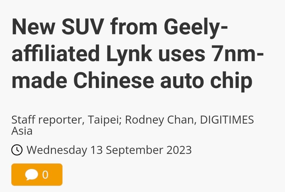
宝贝,让我告诉你另一个消息(图文:吉利旗下领克的新款SUV使用了7纳米中国制造的汽车芯片)
Dalit -> TriptiD
Why are you begging for proof? As if that is going to get Kashmir back.
你为什么在乞求证据?好像这样就能夺回克什米尔似的。
GreatHanWarrior -> Dalit
India = joke.
印度 = 笑话。
kuge -> GreatHanWarrior
actually 7nm or even 5nm can be made with DUV with multiple patterning but costly.
it is just uncertain china fabbed them with domestic equip or not.
实际上,7 纳米甚至 5 纳米都可以通过 DUV 多重图案化技术实现,但成本高昂。
只是不确定中国是否用国产设备制造了这些芯片。
GreatHanWarrior -> kuge
It is Huawei's patented technology. It's not about using “Western technology at a high cost”.
The EUV Litography System was currently created exclusively by Dutch company ASML and filed a similar patent (US2016007434A1) in 2016 but has a different scope of patents. ASML is not allowed to sell the machine to China.
The difference between the two patents is that Huawei uses a rotating illumination device to reduce the number of bright or dark patterns in the same area. It seems that Huawei really wants to overcome the vacancy in the EUV Litography market.
As EUV discovery helped bring chips to 7nm and lower process nodes, Huawei patents could help China's Semiconductor Manufacturing International Corporation (SMIC) ultimately compete with TSMC and Samsung Foundry
这是华为的专利技术。而不是“高成本地使用西方技术”。
EUV光刻系统目前由荷兰公司ASML独家研发,并于2016年申请了类似专利(US2016007434A1),但专利范围不同。ASML公司不被允许向中国销售该设备。这两项专利的不同之处在于,华为使用了旋转照明装置,以减少同一区域内明暗图案的数量。看来,华为真的想克服 EUV 光刻市场的空缺。
由于 EUV 的发现有助于将芯片带入7纳米和更精细的工艺节点,华为的专利可以帮助中国中芯国际最终与台积电和三星晶圆厂竞争。
TriptiD -> GreatHanWarrior
You are an idiot. I am putting you an ignore.
It is well documented that SMIC has produced the 7 nm chips using multiple rounds of patterning using DUV technology. TSMC used the same process before the advent or EUV, but the yield is very poor and the cost of the chip using this process could be 10x the cost using EUV.
The DUV machines being used by SMIC are most likely either from ASML or Nikon.
你这个白痴,我完全无视你。
有充分的资料显示,中芯国际利用DUV技术通过多重图案化生产出了7纳米芯片。台积电在EUV出现之前也采用了同样的工艺,但产量很低,采用这种工艺的芯片成本可能是采用EUV工艺的 10 倍。
中芯国际使用的DUV光刻机很可能来自ASML或尼康。
Han Patriot -> TriptiD
You need to chill bro. Nobody knows which process was used and nobody even knows it was a loss as you said. Nobody is stupid enough to make 40mil phones for a loss. If it is indeed SMIC, Mr. Liang the Chinese from Taiwan aka Taiwanese found a way to scale it up and improve the yield.
There is news coming out that SMIC Duvs can't satisfy 40mil chips and SSA800 is already running and producing. It's up to you to believe what you want but just because India can't make it doesn't mean they can't.
兄弟,你需要冷静一下。没有人知道使用了哪种工艺,甚至没有人知道是不是像你说的那样亏损。没有人会傻到亏本生产4000万部手机。如果真的是中芯国际,那么来自台湾的中国人(或者台湾人)梁先生找到了扩大规模和提高产量的方法。
有两条消息“中芯国际的DUV无法满足4000万芯片的需求”,“中国的SSA800光刻机已经在运行和生产”。你想相信哪个由你决定,但印度做不出来并不意味着他们做不出来。
TriptiD -> Han Patriot
No one knows for sure because neither SMIC nor Huawei has spoken about it, but there is plenty of circumstantial evidence that DUV process with multiple patterning was used.
由于中芯国际和华为都没有提及此事,所以没有人知道确切的情况,但有大量间接证据表明,是使用了具有多重图案化的DUV工艺。
Han Patriot -> TriptiD
The point is you benchmark yourself to India. A few years ago nobody believed China could make advanced turbofans.
关键是你以印度为基准。几年前,没人相信中国能制造出先进的涡扇发动机。
GreatHanWarrior -> TriptiD
You are a hopeless little idiot.
Return to a common sense question. If you use ASML/Nikon to produce chips, Americans won't know????
I have enough evidence. If you use ASML to produce 7nm chips. Americans will immediately remotely shut down all EUV/DUVs!
你真是个无可救药的小白痴。
回到一个常识性的问题。如果用ASML/尼康生产芯片,美国人会不知道???
我有足够的证据。如果你用ASML来生产7纳米芯片。美国人会立即远程关闭所有的EUV/DUV!
Menthol -> MH.Yang
I can't wait to see Huawei launching 5mn chip and so on.
我迫不及待地想看到华为推出5纳米的芯片等。
Menthol -> MH.Yang
I think China technology advancement is no longer tied to the West. Instead of trailing behind or collaborating, China is able to take another path.
Since China research is already the world biggest, that explain everything.
我觉得中国的技术进步不再与西方联系在一起了。不是落后或合作,中国有能力另辟蹊径。
由于中国的研究已经是世界最大的,这就说明了一切。
MH.Yang
BTW: According to experts in the field, if synchrotron radiation technology is used, it can achieve a 1NM effect with a 7NM stack, with the drawback of only a slightly higher heat generation.
Such a factory is something that only China is capable of building. Not only does it require a lot of industrial support and a lot of capital investment, it also has a lot of unique technologies and patents in the hands of Chinese state-owned enterprises. For example, 100,000 KW of power needs to be transmitted by ultra-high voltage, which is a unique technology and patent of China's power grid. The vast majority of countries, including the United States, do not have ultra-high voltage power grids, and China is the only country that has the ability to build such a plant.
顺便一提:据该领域的专家称,如果使用同步辐射技术,可以用7纳米的堆栈实现1纳米的效果,缺点是发热量稍高。
这样的光刻工厂只有中国才有能力建造。它不仅需要大量的产业配套和大量的资金投入,而且中国国有企业还掌握着许多独特的技术和专利。例如,10万千瓦的电力需要通过特高压输送,这是中国电网的独有技术和专利。包括美国在内的绝大多数国家都没有特高压电网,只有中国有能力建设这样的电厂。
Han Patriot -> MH.Yang
Theoretically it is possible since weakness is in shrinking the component size. They are compensating this by using another approach. Instead of killing a mosquito with a small tennis racquet, using a big racquet the size of a room.
从理论上讲,这是可能的,因为劣势在于缩小组件的尺寸。他们正在用另一种方法来弥补这一劣势。不是用小网球拍来拍死蚊子,而是用一个房间大小的大球拍。
MH.Yang -> Han Patriot
Some people know very well that the Chinese Government is very far-sighted and often engages in very long-term planning. But they still believe that Beijing was not ready to deal with the semiconductor issue until the United States launched sanctions.
Some know that China is the only country with a complete industrial chain, and that its industrial scale and research capabilities are much larger than those of the Netherlands. But they still believe that China will use the same methods as the Netherlands to manufacture semiconductors.
有些人很清楚,中国政府是很有远见的,经常进行非常长远的规划。但他们仍然认为,在美国发起制裁之前,中国政府还没有做好处理半导体问题的准备。
有些人知道,中国是唯一一个拥有完整产业链的国家,其工业规模和研究能力远远超过荷兰。但他们仍然认为,中国将采用与荷兰相同的方法来生产半导体。
Menthol -> MH.Yang
Yes, based on my observation for years, China government is far sighted and do long term planning.
It's always went to the basic first, then stepping the ladder one by one.
Chinese government is also love to do social and economic experience, like setting up special zones with special social and economic policies. If it's successful, then it will be implemented national wide.
是的,根据我多年的观察,中国政府很有远见,会做长远规划。
它总是先从基础做起,然后再一步一步往上爬。
中国政府也很喜欢做社会和经济方面的尝试,比如设立特区,实行特殊的社会和经济政策。如果成功了,就会在全国范围内推行。
Han Patriot -> MH.Yang
This will buy time to miniturize the components further. Coupled with chiplet tech, Huawei has a big chance to win this race.
这将为进一步微型化组件赢得时间。再加上芯片技术,华为有很大机会赢得这场竞赛。
CIA Mole -> Han Patriot
China is 100% reactive and not proactive, unable to see anything coming from sanctions to covid to economy
中国完全是被动的,而没有主动,从制裁到新冠疫情再到经济,它什么都看不到
艹艹艹
Recent progress of SSMB EUV light source project at Tsinghua University
https://conference-indico.kek.jp/event/160/contributions/2876/attachments/2148/2699/Zhilong_Pan.pdf
清华大学 SSMB 超紫外光源项目的最新进展(注:专业内容很长,需要的可以自行查看以上链接)
Menthol -> 艹艹艹
"In relatively low price"
Again, every time I read China research report, I see a lot the words of "low price".
It's truly helping humanity, improving everyone's standard of living.
“价格相对较低”
又看到了,每次我读中国的研究报告时,都会看到很多“价格低”的字眼。
它确实在帮助人类,提高每个人的生活水平。
mmr
Will it reduce cost for everything in future?
Any innovation is good Innovation.
这是否会降低今后一切东西的成本?
任何创新都是好的创新。
MH.Yang -> mmr
Any area where China joins in will result in a price dafu drop.
中国参与的任何领域都会导致价格大跌。
KB
Okay
This is highly exaggerated
In reality, one thought process is that China are MASTERS of upscale and NOVICES of micro scale
So a school of experts feel
Why should we spend all our money on micro scale engineering which was NEVER our expertise
Chinese cracked most of their tough problems by RISING THE SCALE
Now they say rather than to manufacture fine extreme light sources, they already can manufacture immensely powerful light sources on large scale
Likewise they can never make lenses like Zeiss because that's microscale, yet they can make large focal precision optics and be the best in the world at it
Now with such a huge scale, you cannot build EUV machines or mother machines but YOU CAN BUILD A FACTORY!!!
好吧,这太夸张了
实际上,有一种观点认为,中国是大型工程的大师,而微型工程是新手。
所以,有一派专家认为,我们为什么要把所有的钱都花在微型工程上呢,因为这根本就不是我们的专长。
中国人通过放大规模解决了大多数棘手的问题。
现在他们说,与其制造精细的极致光源,不如以大规模制造强力的光源。
同样,他们永远无法制造出像蔡司那样的透镜,因为那是微尺度的,但他们可以制造出大焦距精密光学器件,而且是世界上最好的。
现在在如此巨大的规模下,你无法制造EUV设备或母机,但你可以建造一座工厂!
A Massive Factory that if it works could make Chipmaking the equivalent of an Industry Assembly Line which the Chinese are not just masters but super masters
So you will have factories that will resemble EUV machines churning out 1.6 Billion Chips every time
Of these 80% Chips will be Junk, 15% Chips will be low quality yet 5% Chips will be high yield and great quality
The experts claim that even this 5% which will be cost effective because of the large scale of the process
So far they kept trying to copy the West which are experts on micro scale and precision but suck at upscale today
They treated EUVs like an Engineering Problem and that's not their greatest strength
Now they treat EUVs like a Production problem and thats their greatest strength
Currently this is one of the three routes chosen by China to develop their own cutting edge semiconductors
The other routes include Innovative Stacking processes using DUVs and not needing EUVs at all
And a third route to make EUV’s conventionally
The Timeline is 2027–2030
It's not next year
一座巨大的工厂,如果成功,就能使芯片制造相当于工业装配线,而这方面中国人不仅是大师,而且是超级大师。
因此,你会有类似于EUV机器的工厂,每次都能生产出16亿个芯片。
其中80%的芯片将是垃圾芯片,15%的芯片将是低质量芯片,而5%的芯片将是高产优质芯片。
专家们认为,由于工艺规模庞大,即使是这5%也具有成本效益。
到目前为止,他们一直在试图模仿擅长微观和精确度而大规模工程很糟糕的西方国家。
他们像对待工程问题一样对待EUV,这并不是他们最大的优势。现在,他们把EUV视为生产问题,这也是他们最大的优势所在。目前,这是中国选择发展自己的先进半导体的三条路线之一,其中一条路线包括使用DUV的创新堆叠工艺,完全不需要EUV,第三条路线是以传统方式制造EUV。
时间表是2027-2030年,不是明年。
serenity
We'll have to see if Huawei offers to sells this latest 7nm Kirin chip to other Chinese computer and smartphone makers. This chip is still 2 gen behind TSMC's latest 3nm nodes but of course barely much realistic difference between 7nm and 3nm when the alternative is either 14nm manufacturing or no chips at all.
我们将拭目以待,看看华为是否会向其他中国电脑和智能手机制造商出售这款最新的7纳米麒麟芯片。这款芯片仍然落后于台积电最新的3纳米节点2代。当然,当替代方案要么是14纳米制造工艺,要么是根本没有芯片的时候,7纳米和3纳米之间就几乎没有什么实际差别了。
Bengal71
Even though a solid source is not established here, with the track record of the Chinese I would choose to believe it. I anticipated it coming when the sanctions were applied. Chinese people always defeated sanctions in the past.
My next prediction is China will surpass ASML, TSMC, Samsung and other western tech companies in chip technology, perhaps in the next 3/4 years. What they will continue to lack is google services, they are not trying to develop google like services for global consumers which is a mistake.
尽管这里没有可靠的消息来源,但以中国人的过往记录,我会选择相信它。在实施制裁时,我就预料到会发生这样的事情。在过去,中国人民总是能战胜制裁。
我的下一个预测是,也许在未来3到4年内,中国将在芯片技术方面超过 ASML、台积电、三星和其他西方科技公司。他们将继续缺乏的是谷歌服务,他们没有尝试为全球消费者开发类似谷歌的服务,这是一个失误。
Menthol -> Bengal71
The original plan is use 7nm chip in 2022.
But because of USA sanctions, it was delayed up to the end of 2023.
原计划在 2022 年使用 7 纳米芯片。
但由于美国的制裁,被推迟到 2023 年底。
StraightEdge
I saw this, no idea how much reliable information.
Microbunching illuminates new technological horizon-Tsinghua University www.tsinghua.edu.cn
A scheme that causes electrons to form microbunches’ could yield high power and coherent extreme-ultraviolet light, and perhaps the means to produce circuits faster.A new source of high-power extreme-ultraviolet (EUV) light, steady-state microbunching (SSMB), is peeking over the horizon, following a proof-of-principle experiment published in Nature. Corresponding author, Chuanxiang Tang, says the potential power of SSMB EUV could be used to etch more-intricate patterns onto semiconductor circuits.
我看到了这个,不知道有多少可靠信息。
《清华大学:微束照亮新的技术领域》(链接)
一种能使电子形成微束的方法可以产生高功率和相干的极紫外光,也许还能更快地制造电路。在《自然》发表了一项原理验证实验之后,一种新的高功率极紫外光(EUV)来源——稳态微束(SSMB)初露端倪。通讯作者唐传祥说,SSMB极紫外光的潜在功率可用于在半导体电路上蚀刻更复杂的图案。
Char -> StraightEdge
EUV lithography machines made in China do not need to be portable, and the technical requirements for lenses and photoresists will be reduced.
中国制造的EUV光刻机不需要便携性,对镜头和光刻胶的技术要求也会降低。
Menthol -> StraightEdge
I still don't know whatever Huawei 7nm chip is made using this technique or DUV.
But the news you posted is an idea to fabricate 1nm in the future, even below 1nm.
我还不知道华为7纳米芯片是采用这种技术还是DUV技术制造的。
但你发的链接是一种未来制造1纳米甚至1纳米以下产品的想法。
MH.Yang -> Menthol
Let me explain it this way. There are various sizes of light segments in a beam of light, 12nm, 7nm, 5nm and so on.
ASML's machines need to be transported to Asia, so they are small. ASML's machines are also relatively small in power due to the lack of extra high voltage power grids in countries other than China.
So ASML's machine is limited to intercepting only one size of light segment at a certain frequency segment. For example, a 7nm machine can only intercept a 7nm segment.
China's SSMB-EUV programme takes advantage of China's extra-high voltage grid to provide super-high input power, and it's essentially a lithography machine larger than an aircraft carrier.SSMB-EUV extends the distance of the intercepted light segments dramatically, and depending on the frequency, different sized segments are concentrated at different nodes. Then we can get different sizes of light segments at different nodes to make different sizes of chips. For example, make 24mm at point A, 12nm at point B and so on. This solution can drastically reduce the cost, improve the yield and increase the manufacturing speed.
让我来解释一下吧。一束光中有不同大小的光段,12纳米、7纳米、5纳米等。
ASML的光刻机需要运往亚洲,所以体积很小。由于中国以外的国家没有特高压电网,ASML的机器功率也相对较小。
所以,ASML的光刻机只能在某一频率段截取一种尺寸的光段。例如,7纳米机器只能截取7纳米的光段。
中国的SSMB-EUV计划利用中国的特高压电网,提供超高的输入功率,它实质上是一台比航空母舰还大的光刻机。SSMB-EUV截取光段的距离大大延长了,根据频率的不同,不同大小的光段会集中在不同的节点上。这样,我们就可以在不同的节点获得不同大小的光段,从而制造出不同大小的芯片。例如,在A点制造24毫米的芯片,在B点制造12纳米的芯片,以此类推。这种解决方案可以大大降低成本,提高产量和制造速度。
This large research facility was originally designed for scientific research in the extreme ultraviolet band.
这个大型研究设施最初是为极紫外波段的科学研究而设计的。
Bengal71 -> MH.Yang
Can you please provide some source of this news?
你能提供一些消息来源吗?
Menthol -> MH.Yang
So, it uses a different method.
No wonder Huawei dares enough to release his own chip.
I thought it used DUV tricks.
所以,它采用了不同的方法。
难怪华为敢于发布自己的芯片。
我还以为它是使用了某种DUV技巧。
White and Green with M/S -> MH.Yang
What is the source dude???
消息来源是什么???
Skull and Bones
That is a big innovation.
这是一项重大创新。
MH.Yang
Due to the global division of labour, if photolithography is too large to be transported from Europe to Asia, so the semiconductor industry is now using ASML's compact lithography technology.
The SSMB-EUV light source used in China has an output power of >100000KW, a capacity 40 times that of ASML, an accelerator length of >200 metres and a width of >20 metres alone, and it is capable of using dozens of EUVs at the same time with a beam splitter. The whole SSMB-EUV light source volume is equivalent to a photolithography factory. The construction of SSMB-EUV light source requires a complete industrial chain and huge capital investment, and China is the only country that can meet all the conditions.
由于全球分工,如果光刻机体积太大,就无法从欧洲运到亚洲,因此半导体行业现在使用的是 ASML 的紧凑型光刻技术。
中国使用的SSMB-EUV光源输出功率大于100000千瓦,功率是ASML的40倍,加速器长度大于200米,仅宽度就大于20米,通过分束器可以同时使用几十台EUV的能力。整个SSMB-EUV光源体积相当于一座光刻工厂。建设SSMB-EUV光源需要完整的产业链和巨大的资金投入,而中国是唯一能够满足所有条件的国家。
TriptiD
Source of this news ? What is the unit cost of chips manufactured using this technique?
新闻来源?使用这种技术制造芯片的单位成本是多少?
ziaulislam -> TriptiD
Cost...it's weird when talk about cost when it comes to China manufacturing thing
The question has been asked since 1990s and we deep down have always known the answer
Sooner or later China will get it done like it has always been the case
成本......当谈到中国制造的成本时,感觉很奇怪
这个问题自90年代就一直被问到,而我们内心深处始终都知道答案
中国迟早会像以往一样实现这项成就
TriptiD -> ziaulislam
We are not talking about t-shirts and towels here.
The reason that I am asking about costs is that the chips could have been made using new tech in an experimental setting- which could be prohibitively expensive in a commerical setting. For example, you can "manufacture " gold in a particle accelerator, but the cost is prohibitive.
我们不是在讨论T恤和毛巾。
我之所以要问成本问题,是因为这些芯片可能是在实验环境中,使用新技术制造的——在商业环境中,这种技术的成本可能高得令人望而却步。例如,你可以用粒子加速器“制造”黄金,但成本高得离谱。
ziaulislam -> TriptiD
No we are talking about solar panels and other electronics costs
Ultimately China will figure out how to decrease the cost
They always do
不,我们说的是太阳能电池板和其他电子产品的成本
中国最后都会想办法降低成本,他们总是这样做
epebble -> TriptiD
That question is easy to answer. If they sell only 100,000 7nm chips, your suspicion may be correct. But if they sell 100 million 7nm chips, they could not be making it at a loss and survive. In 2022, 1,400 million smartphones were sold. So, 100 million is only 7% of smartphones market.
这个问题很容易回答。如果他们只卖出10万片7纳米芯片,你的怀疑可能是正确的。但如果他们卖出了1亿个7纳米芯片,他们就不可能在亏损的情况下生存下来。2022 年,智能手机的销量为14亿部。所以,1亿只占智能手机市场的7%。
TriptiD -> epebble
Or they could just be using the existing process using ASML machines obtained by busting sanctions and not the technology the OP is claiming. That is why I asked him for the source of the news.
或者,他们可能只是通过打破制裁,使用获得的 ASML 机器的现有工艺,而不是题主所声称的技术。这就是我问他消息来源的原因。
epebble -> TriptiD
Unlikely. Even if they obtain them clandestinely, which is very difficult, as they are huge and enormously expensive and hence easily tracked. It is like surreptitiously buying a 747 or an aircraft carrier, they need huge amount of handholding services from the manufacturer. Imagine a large jet, times 1000. Can you steal this?
The $150 Million Machine Keeping Moore’s Law Alive
不太可能。即使他们秘密获得这些设备,也是非常困难的,因为这些武器体积庞大,价格昂贵,因此很容易被追踪到。这就好比偷偷购买一架 747 或一艘航空母舰,它们需要制造商提供大量的协助服务。想象一下,一架大型喷气式飞机,乘以 1000。你能偷到这个吗?
价值1.5亿美元的机器让摩尔定律得以延续
TriptiD -> epebble
You are forgetting even nations like Pakistan and North Korea have stolen missile and nuclear tech. So, yes, if China is motivated enough , they can definitely get an ASML machine by busting sanctions.
你忘了,就连巴基斯坦和朝鲜这样的国家也曾窃取导弹和核技术。所以,是的,如果中国有足够的动力,他们完全可以通过打破制裁获得 ASML 设备。
GreatHanWarrior -> TriptiD
Usually. Indians are better at these things. And they are proud of it.
通常情况下印度人更擅长这类事情。他们为此感到自豪。
epebble -> TriptiD
Missile and nuclear tech are easier than 7 nm. Neither Pakistan nor NK have high tech. Their roads, railroads and ports -19th Century technology - are built/supplied by China. Their challenge is to run a power grid.
导弹和核技术比7纳米更容易。巴基斯坦和朝鲜都没有高科技。他们的公路、铁路和港口都是19世纪的技术,都是由中国建造/提供的。他们面临的挑战是运行电网。
TriptiD -> epebble
The question was about STEALING, not about whether it is high tech or low tech. If I have enough money and not located in China, I can purchase a ASML machine, but I can't purchase missile or nuclear tech.
And if China has indigenously developed an alternate tech, why is it keeping so quiet about it ? Doesn't it want to boast to the world that it defeated US sanctions and get customers for its indigenous technology?
问题是关于“窃取”,而不是关于“高科技”或“低科技”。如果我有足够的钱,而且不在中国,我可以购买ASML设备,但我不能购买导弹或核技术。
如果中国已经自主研发了替代技术,为什么还要保持沉默?难道它不想向全世界夸耀自己战胜了美国的制裁,并为自己的本土技术争取客户吗?
BT -> TriptiD
None of these are true. Don’t water down China’s achievements in indigenizing semiconductor supply chain with fantasies.
这些都不是真的。不要用幻想来淡化中国在半导体供应链本土化方面取得的成就。
FS -> BT
It’s more BS from the US intelligence. They think that if they make ridiculous statements then no one will believe that China can make 7nm chips.
What the US government and bureaucrats don’t seem to understand is that no amount of BS and hot air can change what is really happening.
It doesn’t matter whether the Western population thinks that China can make 7nm chips or not. China is going to keep making them and build fabs to make them.
For some strange reason, they have replaced reality with propaganda and think that this will do something.
I’m still at a loss as to what they think will happen. No amount of propaganda helped the Nazis when they lost in WWII.
I read an article that the Germans were shocked when allied troops showed up outside Berlin and started hammering the city.
They thought they were winning WWII!
这更像是美国情报部门的胡说八道。他们认为,如果他们发表荒谬的言论,就不会有人相信中国能制造出7纳米芯片。
美国政府和官僚们似乎不明白的是,再多的胡说八道和空谈也无法改变正在发生的真实情况。
西方人是否认为中国能生产7纳米芯片并不重要。中国将继续生产7纳米芯片,并建立生产7纳米芯片的工厂。
出于某种奇怪的原因,他们用宣传取代了现实,并认为这样会有所作为。
我仍然不知道他们认为会发生什么。当纳粹在二战中失败时,再多的宣传也无济于事。
我读过一篇文章,说当盟军部队出现在柏林城外并开始轰炸这座城市时,德国人感到非常震惊。他们还以为自己赢得了二战!
etylo -> TriptiD
Chinese are not boastful like you Indians, don't think every one is like you.
中国人不像你们印度人那样爱吹牛,不要以为每个人都和你们一样。
GreatHanWarrior -> TriptiD
So. Please prove that the Chinese 7nm chip uses ASML EUV.
Please prove. Thank you.
那么请证明中国的7纳米芯片使用的是 ASML 的EUV光刻机。
请证明。谢谢。
beijingwalker -> TriptiD
Funny words from someone whose media produces the most lies in the world.
India has more fake news than any other country in the world
Nearly 60% of Indians had seen fake news against the global average of 57%, said a recent survey. Overall, India ranked seventh in Microsoft’s ‘Digital Civility’
来自一个媒体制造了世界上最多谎言的国家的人,说出一些滑稽的话
印度的假新闻比世界上任何国家都多
最近的一项调查显示,近 60% 的印度人看到过假新闻,而全球平均比例为 57%。总体而言,印度在微软的“数字文明”中排名第七。
TriptiD -> beijingwalker
I have said so many times that I can't prove it because I don't even know if its true.
I am sure Tsinghua is doing some cutting edge research in the field. I doubt that the tech used in the SMIC chips in the Huawei chips is fully Chinese, but if someone presents evidence to that effect, then I will admit my doubts were ill-founded.
My understanding is that until now the known processes for making those chips required ASML machines. I am not saying China has not developed an alternative, only that there is no public records or evidence about what that process is.
我说过很多次,我无法证明它,因为我甚至不知道这是不是真的。
我相信清华正在该领域开展一些前沿研究。我怀疑华为芯片中使用的中芯国际芯片技术是否完全是中国的,但如果有人提出这方面的证据,我会承认我的怀疑是没有根据的。
我的理解是,到目前为止,制造这些芯片的已知工艺需要 ASML 的设备。我并不是说中国没有开发出替代方案,只是没有关于这一过程的公开的记录或证据。
Menthol -> TriptiD
That is the news.
Because Huawei is able to produce 7nm chips without ASML.
And now everyone is investigating and proposing several theories about it.
Up to now, no one really knows the truth.
My theory is probably a DUV trick, as SMIC launched 7nm processor for bitcoin mining using a DUV trick last year.
And it's not a coincidence because Huawei is launching 7nm processor instead of 5nm or 3nm.
这就是新闻。
因为华为能够在没有 ASML 的情况下生产7纳米芯片。
现在,每个人都在对此进行调查并提出了一些理论。
到目前为止,没有人知道真相。
我的推测可能是某种 DUV 技巧,因为中芯国际去年推出的用于比特币挖矿的7纳米处理器就使用了一种DUV技巧。
这并非巧合,因为华为推出的是7纳米处理器,而不是5纳米或3纳米处理器。
GreatHanWarrior -> TriptiD
If India wants to look different from Pakistan. India develops its own technology first!
Currently, even cameras. India still relies on Chinese technology. India and Pakistan are not too different.
如果印度想看起来与巴基斯坦有所不同。印度要先发展自己的技术!
目前,即使是摄像头,印度仍然依赖中国技术。印度和巴基斯坦并没有太大区别。
GreatHanWarrior -> TriptiD
Let me talk about a common sense topic - if Huawei chips use ASML. Americans will know Mate 60 before Chinese people.
The fact is. The ASML owned by China cannot manufacture 7nm chips.
Huawei 7nm chip is completely based on Chinese semiconductor technology!
让我来说一个常识性的话题——如果华为芯片使用的是ASML设备。美国人会比中国人更早知道Mate 60的。
事实是,中国拥有的ASML设备无法生产7纳米芯片。
华为7纳米芯片完全基于中国的半导体技术!
MH.Yang
The news comes from a product launch on 12 September 2023 reported by Huawei. Huawei mentions that they work with the Beijing Synchrotron Radiation Facility, BSF, on chips. Then the Chinese media enquired about its two factories in Xiongan and Shanghai, owned by CGST and Zhangjiang Hi-Tech, that can manufacture 7nm chips via synchrotron radiation.
The Beijing Synchrotron Radiation Facility, BSF, and Tsinghua University have collaborated to propose the SSMB-EUV light source solution (Steady State Microbeam), which overturns the concept of traditional lithography technology by no longer relying on shrinking the light source to improve the quality of the image, but rather, by enlarging and elongating the light source, to achieve the automatic adjustment of the different wavelengths of light, so as to achieve a higher degree of precision.
Of course, all the news now comes from the unofficial media splicing bits and pieces together and making guesses. It has not been confirmed by official organisations such as Huawei or Tsinghua University. I can understand if people don't believe it.
Satellite view of SSMB-EUV light source factory:
In June 2021, the official Chinese government media reported on the completion of the construction of the SSMB-EUV light source factory:
In February 2023, a press release from Tsinghua University's official media stated that the university's SSMB-EUV light source solution and technology had been put to practical use after spending 10 years and had solved a problem that was a major national need in the field of photolithography:
这一消息来自华为公司于2023年9月12日的产品发布会。华为提到,他们与北京同步辐射中心(BSF)合作开发芯片。随后,中国媒体询问了CGST 和张江高科在雄安和上海的两家工厂,这两家工厂可以通过同步辐射生产7纳米芯片。
北京同步辐射中心(BSF)与清华大学合作,提出了 SSMB-EUV 光源方案(稳态微聚束),颠覆了传统光刻技术的概念,不再依靠缩小光源来提高成像质量,而是通过放大和拉长光源,实现不同波长光的自动调节,从而达到更高的精度。
当然,现在所有的消息都来自非官方媒体的拼凑和猜测。华为或清华大学等官方机构并未证实此事。如果人们不相信,我可以理解。
SSMB-EUV 光源工厂卫星图:
2021 年 6 月,中国官方媒体报道了 SSMB-EUV 光源工厂竣工的消息:
2023 年 2 月,清华大学官方媒体发布新闻稿称,该校的 SSMB-EUV 光源方案和技术历经 10 年时间终于投入实际应用,解决了光刻领域的国家重大需求问题:
Menthol -> MH.Yang
I think this project is not related to the current Huawei 7nm chips.
I think this project is aiming for 1nm chips in the future.
There are still several years away for the launching of 1nm chips, there are still a lot of time for China.
I also wonder, what is China progress on the carbon or graphene based chip?
我觉得这个项目与目前的华为7纳米芯片无关。
我认为这个项目的目标是未来的1纳米芯片。
距离推出1纳米芯片还有几年时间,中国还有很多时间。
我还想知道,中国在碳基或石墨烯基芯片方面有什么进展?
FuturePAF -> Menthol
Or some kind of glass based chips?
Intel seems pretty excited about glass substrates
Intel has announced a a glass substrate breakthrough, which will make its future chips faster and more efficient.
或者某种玻璃基芯片?
英特尔似乎对玻璃基板非常感兴趣
英特尔公司宣布了一项玻璃基板突破,这将使其未来的芯片速度更快、效率更高。
TriptiD -> MH.Yang
Thanks for posting this. I have met a lot of really smart Tshingua graduates, so I have great respect for this university. However, the leap from research in a university and commerical production is a big one and your posts don't provide enough authoritative information to demonstrate this has been done. My main concern is what the unit cost of production will be, taking into account capital costs. The chips in the new phone carry the SMIC label. How is SMIC involved in the process you have described ?
谢谢你发布的这篇文章。我见过很多非常聪明的清华毕业生,因此我非常尊重这所大学。但是,从大学研究到商业化生产是一个巨大的飞跃,而你的帖子没有提供足够的权威信息来证明这一点。我主要关心的是,考虑到资本成本,单位生产成本会是多少。新手机中的芯片贴有中芯国际的标签。中芯国际是如何参与你所描述的过程的?
MH.Yang -> TriptiD
The two plants belong to CGST and Zhangjiang Hi-Tech, two companies under the Beijing Synchrotron Radiation Facility, BSF.
Huawei announced and thanked Beijing Synchrotron Radiation Facility, BSF for their cooperation on the chips at the conference.
Tsinghua University submitted and announced the theory and proposal of SSMB-EUV 10 years ago, and Tsinghua University announced the successful construction of SSMB-EUV factory in February this year.
In February this year, the Chinese government media announced that Beijing Synchrotron Radiation Facility, BSF had built two factories using Tsinghua University's technology and proposal.
Do you see the connection and logic between these events?
这两家工厂属于 CGST 和张江高科,它们是北京同步辐射设施(BSF)下属的两家公司。
华为在会上宣布并感谢北京同步辐射中心(BSF)在芯片方面的合作。
10 年前,清华大学提交并公布了 SSMB-EUV 的理论和方案,今年 2 月,清华大学宣布 SSMB-EUV 工厂建设成功。
今年 2 月,中国政府媒体宣布,北京同步辐射设施(BSF)已利用清华大学的技术和方案建造了两座工厂。
你看到这些事件之间的联系和逻辑了吗?
TriptiD -> MH.Yang
Well, there is some connection but still lot of unanswered questions. How is SMIC involved in all this ? It is their name on the chip, after all. Which entity owns the IP ? Have relevant patents been filed in China ? By whom? And what about the US and other Western countries ? Wouldn't whichever Chinese entity made the breakthrough? Then why hasn't anyone in the West spotted these patent applications yet ?
这两者有一定的联系,但仍有许多问题没有得到解答。中芯国际是如何参与这一切的?毕竟芯片上有他们的名字。哪个实体拥有知识产权?相关专利是否已在中国申请?由谁申请?美国和其他西方国家呢?哪个中国实体取得了突破?为什么西方还没有人发现这些专利申请?
GreatHanWarrior -> TriptiD
Sorry. I don't know what you're being stubborn about.
A new Huawei chip packaging patent reveals performance verification technology
China’s patent office recently published a new Huawei chip packaging technology patent with application number CN116547791A. The title is “a chip package and a Method for preparing chip package”. It was applied on December 16, 2020, and approved on August 4th, 2023.
If India wants to look different from Pakistan. Firstly, India should address the illiteracy issues
不好意思,我不知道你在固执什么。
《一项新的华为芯片封装专利揭示了性能验证技术》(链接)
中国专利局最近公布了一项新的华为芯片封装技术专利,申请号为 CN116547791A。专利名称为“一种芯片封装和制备芯片封装的方法”。该专利于 2020 年 12 月 16 日提出申请,并于 2023 年 8 月 4 日获得批准。如果印度想与巴基斯坦有所不同。印度应该先解决文盲问题。
TriptiD -> GreatHanWarrior
This is a Chinese patent that was applied for in 2020. Huawei probably has hundreds if not thousands of chip-related patents . Are you saying the one you have posted this patents the process that was used to make the SMIC chips on the new Huawei phone ? So, Huawei has had the process since before 2020 ? Why is SMIC's name on the chip if the IP belongs to Huawei?
这是 2020 年申请的一项中国专利。华为可能拥有成百上千项与芯片相关的专利。你是说,你贴出的这项专利就是用于制造华为新手机上中芯国际芯片的工艺吗?那么,华为在 2020 年之前就已经拥有了这一工艺?如果知识产权属于华为,为什么芯片上会有中芯国际的名字?
GreatHanWarrior -> TriptiD
What are you being stubborn about?
Huawei patents EUV lithography tools used to make
Huawei has patented one component used in EUV lithography systems that is required to make high-end processors on sub-10 nm nodes. It solves the problem of interference patterns created by the ultraviolet light that would otherwise make the wafer uneven.
你到底在固执什么?
《华为用于制造超紫外光刻工具的专利》(链接)
华为已为用于超紫外光刻系统的一个组件申请了专利,该组件是在 10 纳米以下节点制造高端处理器所必需的。它解决了紫外光产生的干涉图案问题,否则紫外光会使晶片不平整。
GreatHanWarrior -> TriptiD
The fact is. The ASML owned by China cannot manufacture 7nm chips!
Can you understand?
事实就是,中国拥有的ASML设备无法生产出7纳米芯片!
你能理解吗?
GreatHanWarrior -> TriptiD
Huawei EUV Scanner Patent Suggests Sub-7nm Chips for China
https://www.tomshardware.com/news/huawe-euv-scanner
Huawei has filed a patent application covering an extreme ultraviolet (EUV) lithography scanner, according to UDN. If the company builds such a scanner and achieves decent productivity, uptime, and yields, Chinese chipmakers could produce chips on sub-7nm-class technologies. The only question is when.
In mid-November, Huawei filed an application with the State Intellectual Property Office for a patent covering an EUV scanner and its key components. The patent application number is 202110524685X, reports MyDrivers.
The patent application appears to cover all crucial components of an EUV scanner, including a 13.5 nm EUV light generator (light source), a set of reflecting mirrors, the lithography system, and 'control management technologies' (we would speculate that this is how they call metrology), according to descrlptions published by various media sources.
《华为超紫外扫描仪专利表明中国将采用 7 纳米以下芯片》(链接)
据 UDN 报道,华为已提交了一份关于极紫外(EUV)光刻扫描仪的专利申请。如果该公司能制造出这样的扫描仪,并实现良好的生产率、正常运行时间和产量,那么中国的芯片制造商就能利用 7 纳米以下的技术生产芯片。唯一的问题是什么时候。
11 月中旬,华为向国家知识产权局提交了一份专利申请,内容涉及 EUV 扫描仪及其关键部件。据 MyDrivers 报道,专利申请号为 202110524685X。根据各种媒体发布的描述,该专利申请似乎涵盖了 EUV 扫描仪的所有关键部件,包括 13.5 纳米 EUV 光发生器(光源)、一组反射镜、光刻系统和“控制管理技术”(我们推测这是他们对计量的称呼)。
TriptiD -> GreatHanWarrior
Thanks for the link. No one doubts China is making progress on EUV but so far, until it becomes clear how the SMIC chips were produced, there is no evidence it has succeeded in doing so on an industrial scale.
谢谢你提供的链接。没有人怀疑中国在超紫外光(EUV)方面取得了进展,但迄今为止,在中芯国际芯片的生产方式弄清楚之前,没有证据表明中国在工业规模上取得了成功。
MH.Yang -> TriptiD
You don't seem to be aware that SMIC is under the same sanctions as Huawei. SMIC breaking 7nm represents the same thing as Huawei breaking 7nm.
你似乎不知道中芯国际和华为一样受到制裁。中芯国际突破 7 纳米制程与华为突破 7 纳米制程是一回事。
TriptiD -> MH.Yang
They are both sanctioned but the list of sanctions on them is different. Unless you are saying that in China, the corporate structure and is just a sham and intellectual property of Huawei can be freely handed over to SMIC on the orders of the CCP, then the two entities are distinct and a Huawei product is not the same as a SMIC product.
Anyway, if you see a Reuters link I posted earlier, some analysts think that the 7nm chips were produced through DUV at very low yields. Western companies wouldn't do this because it is not economical but it seems Huawei had no other option and does not mind eating the loss.
它们都受到制裁,但制裁名单不同。除非你是说在中国,华为的公司结构只是一个假象,华为的知识产权可以根据中共的命令随意移交给中芯国际,否则这两个实体是不同的,华为的产品和中芯国际的产品也是不同的。
总之,如果你看到我之前发布的路透社链接,一些分析师认为7纳米芯片是通过DUV以极低的产量生产出来的。西方公司不会这么做,因为这不经济,但华为似乎别无选择,而且不介意承担损失。
GreatHanWarrior -> TriptiD
When Huawei humiliates you with technology. You can only talk about CCP.
Not surprisingly. What a desperate attempt.
当华为用技术羞辱你的时候。你就只能拿中共来说事了。
这并不奇怪。真是绝望的举动。
Dalit -> GreatHanWarrior
These Indians are assholes.
这些印度人都是蠢货。
kuge -> TriptiD
i think china has its own duv machine SSA800.
我认为中国有自己的DUV光刻机SSA800。
GreatHanWarrior -> TriptiD
Think about it, when Huawei started selling Mate 70. How hopeless are you?
想想看,当华为开始销售 Mate 70 时。你会有多绝望?
DoTell -> TriptiD
Thanks for your concern for Huawei's loss
https://defence.pk/threads/huawei-pays-out-us-9-65-billion-in-dividends-to-current-and-retired-staff.739304/
Huawei pays out US$9.65 billion in dividends to current and retired staff
Some 131,507 current and former workers are involved in the shareholder scheme, according to the company’s 2021 annual report
Huawei is 100-per cent owned by employees, including its founder Ren Zhengfei, in a structure that turns eligible employees into stakeholders
谢谢你对华为损失的关心
华为向在职和退休员工支付了 96.5 亿美元的股息(链接)
根据该公司2021年年报,约有131,507名在职和退休员工参与了股东计划
华为的股权由其员工(包括其创始人任正非)100%持有,这种结构将符合条件的员工转变为股东
TriptiD -> DoTell
Everyone knows Huawei is highly profitable. That is why they can afford to make the 7 nm chips using an uneconomical process and sell some smartphones at a loss.
众所周知,华为利润丰厚。这就是为什么他们能承受使用不经济的工艺制造7纳米芯片,并亏本销售一些智能手机。
DoTell -> TriptiD
"Everyone knows"? Is BBC someone? Does BusinssInsider.com know? Where would we have been without the guidance of you geniuses?
“众所周知”?是指BBC的谁吗?BusinssInsider.com知道吗?如果没有你们这些天才的指导,我们将何去何从?
GreatHanWarrior -> TriptiD
Continue to roar. The cars made by Huawei make you even more desperate.
New Wenjie M7 model system is as smooth as Mate 60 Pro, says Huawei
继续嘴硬吧。华为制造的汽车会让你更绝望。
华为表示,新的问界M7车型系统跟Mate 60 Pro一样流畅
TriptiD -> GreatHanWarrior
Do you have any proof that the chips is the Huawei phone were made using Chinese machines instead of DUV/EUV machines that were imported earlier ?
你有证据证明华为手机的芯片是用中国光刻机,而不是早先进口的DUV/EUV光刻机制造的吗?
GreatHanWarrior -> TriptiD
How many times do I need to say it?
The EUV/DUV sold by ASML to China cannot produce 7nm chips!!!
Only Huawei has the technology to produce chips without using ASML products!
Can you understand human language?
Baby. Let me tell you another news.
我还要说多少遍?
ASML出售给中国的EUV/DUV光刻机无法生产 7纳米芯片!
只有华为拥有不使用ASML产品生产芯片的技术!
你听得懂人话吗?
宝贝,让我告诉你另一个消息(图文:吉利旗下领克的新款SUV使用了7纳米中国制造的汽车芯片)
Dalit -> TriptiD
Why are you begging for proof? As if that is going to get Kashmir back.
你为什么在乞求证据?好像这样就能夺回克什米尔似的。
GreatHanWarrior -> Dalit
India = joke.
印度 = 笑话。
kuge -> GreatHanWarrior
actually 7nm or even 5nm can be made with DUV with multiple patterning but costly.
it is just uncertain china fabbed them with domestic equip or not.
实际上,7 纳米甚至 5 纳米都可以通过 DUV 多重图案化技术实现,但成本高昂。
只是不确定中国是否用国产设备制造了这些芯片。
GreatHanWarrior -> kuge
It is Huawei's patented technology. It's not about using “Western technology at a high cost”.
The EUV Litography System was currently created exclusively by Dutch company ASML and filed a similar patent (US2016007434A1) in 2016 but has a different scope of patents. ASML is not allowed to sell the machine to China.
The difference between the two patents is that Huawei uses a rotating illumination device to reduce the number of bright or dark patterns in the same area. It seems that Huawei really wants to overcome the vacancy in the EUV Litography market.
As EUV discovery helped bring chips to 7nm and lower process nodes, Huawei patents could help China's Semiconductor Manufacturing International Corporation (SMIC) ultimately compete with TSMC and Samsung Foundry
这是华为的专利技术。而不是“高成本地使用西方技术”。
EUV光刻系统目前由荷兰公司ASML独家研发,并于2016年申请了类似专利(US2016007434A1),但专利范围不同。ASML公司不被允许向中国销售该设备。这两项专利的不同之处在于,华为使用了旋转照明装置,以减少同一区域内明暗图案的数量。看来,华为真的想克服 EUV 光刻市场的空缺。
由于 EUV 的发现有助于将芯片带入7纳米和更精细的工艺节点,华为的专利可以帮助中国中芯国际最终与台积电和三星晶圆厂竞争。
TriptiD -> GreatHanWarrior
You are an idiot. I am putting you an ignore.
It is well documented that SMIC has produced the 7 nm chips using multiple rounds of patterning using DUV technology. TSMC used the same process before the advent or EUV, but the yield is very poor and the cost of the chip using this process could be 10x the cost using EUV.
The DUV machines being used by SMIC are most likely either from ASML or Nikon.
你这个白痴,我完全无视你。
有充分的资料显示,中芯国际利用DUV技术通过多重图案化生产出了7纳米芯片。台积电在EUV出现之前也采用了同样的工艺,但产量很低,采用这种工艺的芯片成本可能是采用EUV工艺的 10 倍。
中芯国际使用的DUV光刻机很可能来自ASML或尼康。
Han Patriot -> TriptiD
You need to chill bro. Nobody knows which process was used and nobody even knows it was a loss as you said. Nobody is stupid enough to make 40mil phones for a loss. If it is indeed SMIC, Mr. Liang the Chinese from Taiwan aka Taiwanese found a way to scale it up and improve the yield.
There is news coming out that SMIC Duvs can't satisfy 40mil chips and SSA800 is already running and producing. It's up to you to believe what you want but just because India can't make it doesn't mean they can't.
兄弟,你需要冷静一下。没有人知道使用了哪种工艺,甚至没有人知道是不是像你说的那样亏损。没有人会傻到亏本生产4000万部手机。如果真的是中芯国际,那么来自台湾的中国人(或者台湾人)梁先生找到了扩大规模和提高产量的方法。
有两条消息“中芯国际的DUV无法满足4000万芯片的需求”,“中国的SSA800光刻机已经在运行和生产”。你想相信哪个由你决定,但印度做不出来并不意味着他们做不出来。
TriptiD -> Han Patriot
No one knows for sure because neither SMIC nor Huawei has spoken about it, but there is plenty of circumstantial evidence that DUV process with multiple patterning was used.
由于中芯国际和华为都没有提及此事,所以没有人知道确切的情况,但有大量间接证据表明,是使用了具有多重图案化的DUV工艺。
Han Patriot -> TriptiD
The point is you benchmark yourself to India. A few years ago nobody believed China could make advanced turbofans.
关键是你以印度为基准。几年前,没人相信中国能制造出先进的涡扇发动机。
GreatHanWarrior -> TriptiD
You are a hopeless little idiot.
Return to a common sense question. If you use ASML/Nikon to produce chips, Americans won't know????
I have enough evidence. If you use ASML to produce 7nm chips. Americans will immediately remotely shut down all EUV/DUVs!
你真是个无可救药的小白痴。
回到一个常识性的问题。如果用ASML/尼康生产芯片,美国人会不知道???
我有足够的证据。如果你用ASML来生产7纳米芯片。美国人会立即远程关闭所有的EUV/DUV!
Menthol -> MH.Yang
I can't wait to see Huawei launching 5mn chip and so on.
我迫不及待地想看到华为推出5纳米的芯片等。
Menthol -> MH.Yang
I think China technology advancement is no longer tied to the West. Instead of trailing behind or collaborating, China is able to take another path.
Since China research is already the world biggest, that explain everything.
我觉得中国的技术进步不再与西方联系在一起了。不是落后或合作,中国有能力另辟蹊径。
由于中国的研究已经是世界最大的,这就说明了一切。
MH.Yang
BTW: According to experts in the field, if synchrotron radiation technology is used, it can achieve a 1NM effect with a 7NM stack, with the drawback of only a slightly higher heat generation.
Such a factory is something that only China is capable of building. Not only does it require a lot of industrial support and a lot of capital investment, it also has a lot of unique technologies and patents in the hands of Chinese state-owned enterprises. For example, 100,000 KW of power needs to be transmitted by ultra-high voltage, which is a unique technology and patent of China's power grid. The vast majority of countries, including the United States, do not have ultra-high voltage power grids, and China is the only country that has the ability to build such a plant.
顺便一提:据该领域的专家称,如果使用同步辐射技术,可以用7纳米的堆栈实现1纳米的效果,缺点是发热量稍高。
这样的光刻工厂只有中国才有能力建造。它不仅需要大量的产业配套和大量的资金投入,而且中国国有企业还掌握着许多独特的技术和专利。例如,10万千瓦的电力需要通过特高压输送,这是中国电网的独有技术和专利。包括美国在内的绝大多数国家都没有特高压电网,只有中国有能力建设这样的电厂。
Han Patriot -> MH.Yang
Theoretically it is possible since weakness is in shrinking the component size. They are compensating this by using another approach. Instead of killing a mosquito with a small tennis racquet, using a big racquet the size of a room.
从理论上讲,这是可能的,因为劣势在于缩小组件的尺寸。他们正在用另一种方法来弥补这一劣势。不是用小网球拍来拍死蚊子,而是用一个房间大小的大球拍。
MH.Yang -> Han Patriot
Some people know very well that the Chinese Government is very far-sighted and often engages in very long-term planning. But they still believe that Beijing was not ready to deal with the semiconductor issue until the United States launched sanctions.
Some know that China is the only country with a complete industrial chain, and that its industrial scale and research capabilities are much larger than those of the Netherlands. But they still believe that China will use the same methods as the Netherlands to manufacture semiconductors.
有些人很清楚,中国政府是很有远见的,经常进行非常长远的规划。但他们仍然认为,在美国发起制裁之前,中国政府还没有做好处理半导体问题的准备。
有些人知道,中国是唯一一个拥有完整产业链的国家,其工业规模和研究能力远远超过荷兰。但他们仍然认为,中国将采用与荷兰相同的方法来生产半导体。
Menthol -> MH.Yang
Yes, based on my observation for years, China government is far sighted and do long term planning.
It's always went to the basic first, then stepping the ladder one by one.
Chinese government is also love to do social and economic experience, like setting up special zones with special social and economic policies. If it's successful, then it will be implemented national wide.
是的,根据我多年的观察,中国政府很有远见,会做长远规划。
它总是先从基础做起,然后再一步一步往上爬。
中国政府也很喜欢做社会和经济方面的尝试,比如设立特区,实行特殊的社会和经济政策。如果成功了,就会在全国范围内推行。
Han Patriot -> MH.Yang
This will buy time to miniturize the components further. Coupled with chiplet tech, Huawei has a big chance to win this race.
这将为进一步微型化组件赢得时间。再加上芯片技术,华为有很大机会赢得这场竞赛。
CIA Mole -> Han Patriot
China is 100% reactive and not proactive, unable to see anything coming from sanctions to covid to economy
中国完全是被动的,而没有主动,从制裁到新冠疫情再到经济,它什么都看不到
艹艹艹
Recent progress of SSMB EUV light source project at Tsinghua University
https://conference-indico.kek.jp/event/160/contributions/2876/attachments/2148/2699/Zhilong_Pan.pdf
清华大学 SSMB 超紫外光源项目的最新进展(注:专业内容很长,需要的可以自行查看以上链接)
Menthol -> 艹艹艹
"In relatively low price"
Again, every time I read China research report, I see a lot the words of "low price".
It's truly helping humanity, improving everyone's standard of living.
“价格相对较低”
又看到了,每次我读中国的研究报告时,都会看到很多“价格低”的字眼。
它确实在帮助人类,提高每个人的生活水平。
mmr
Will it reduce cost for everything in future?
Any innovation is good Innovation.
这是否会降低今后一切东西的成本?
任何创新都是好的创新。
MH.Yang -> mmr
Any area where China joins in will result in a price dafu drop.
中国参与的任何领域都会导致价格大跌。
KB
Okay
This is highly exaggerated
In reality, one thought process is that China are MASTERS of upscale and NOVICES of micro scale
So a school of experts feel
Why should we spend all our money on micro scale engineering which was NEVER our expertise
Chinese cracked most of their tough problems by RISING THE SCALE
Now they say rather than to manufacture fine extreme light sources, they already can manufacture immensely powerful light sources on large scale
Likewise they can never make lenses like Zeiss because that's microscale, yet they can make large focal precision optics and be the best in the world at it
Now with such a huge scale, you cannot build EUV machines or mother machines but YOU CAN BUILD A FACTORY!!!
好吧,这太夸张了
实际上,有一种观点认为,中国是大型工程的大师,而微型工程是新手。
所以,有一派专家认为,我们为什么要把所有的钱都花在微型工程上呢,因为这根本就不是我们的专长。
中国人通过放大规模解决了大多数棘手的问题。
现在他们说,与其制造精细的极致光源,不如以大规模制造强力的光源。
同样,他们永远无法制造出像蔡司那样的透镜,因为那是微尺度的,但他们可以制造出大焦距精密光学器件,而且是世界上最好的。
现在在如此巨大的规模下,你无法制造EUV设备或母机,但你可以建造一座工厂!
A Massive Factory that if it works could make Chipmaking the equivalent of an Industry Assembly Line which the Chinese are not just masters but super masters
So you will have factories that will resemble EUV machines churning out 1.6 Billion Chips every time
Of these 80% Chips will be Junk, 15% Chips will be low quality yet 5% Chips will be high yield and great quality
The experts claim that even this 5% which will be cost effective because of the large scale of the process
So far they kept trying to copy the West which are experts on micro scale and precision but suck at upscale today
They treated EUVs like an Engineering Problem and that's not their greatest strength
Now they treat EUVs like a Production problem and thats their greatest strength
Currently this is one of the three routes chosen by China to develop their own cutting edge semiconductors
The other routes include Innovative Stacking processes using DUVs and not needing EUVs at all
And a third route to make EUV’s conventionally
The Timeline is 2027–2030
It's not next year
一座巨大的工厂,如果成功,就能使芯片制造相当于工业装配线,而这方面中国人不仅是大师,而且是超级大师。
因此,你会有类似于EUV机器的工厂,每次都能生产出16亿个芯片。
其中80%的芯片将是垃圾芯片,15%的芯片将是低质量芯片,而5%的芯片将是高产优质芯片。
专家们认为,由于工艺规模庞大,即使是这5%也具有成本效益。
到目前为止,他们一直在试图模仿擅长微观和精确度而大规模工程很糟糕的西方国家。
他们像对待工程问题一样对待EUV,这并不是他们最大的优势。现在,他们把EUV视为生产问题,这也是他们最大的优势所在。目前,这是中国选择发展自己的先进半导体的三条路线之一,其中一条路线包括使用DUV的创新堆叠工艺,完全不需要EUV,第三条路线是以传统方式制造EUV。
时间表是2027-2030年,不是明年。
serenity
We'll have to see if Huawei offers to sells this latest 7nm Kirin chip to other Chinese computer and smartphone makers. This chip is still 2 gen behind TSMC's latest 3nm nodes but of course barely much realistic difference between 7nm and 3nm when the alternative is either 14nm manufacturing or no chips at all.
我们将拭目以待,看看华为是否会向其他中国电脑和智能手机制造商出售这款最新的7纳米麒麟芯片。这款芯片仍然落后于台积电最新的3纳米节点2代。当然,当替代方案要么是14纳米制造工艺,要么是根本没有芯片的时候,7纳米和3纳米之间就几乎没有什么实际差别了。
Bengal71
Even though a solid source is not established here, with the track record of the Chinese I would choose to believe it. I anticipated it coming when the sanctions were applied. Chinese people always defeated sanctions in the past.
My next prediction is China will surpass ASML, TSMC, Samsung and other western tech companies in chip technology, perhaps in the next 3/4 years. What they will continue to lack is google services, they are not trying to develop google like services for global consumers which is a mistake.
尽管这里没有可靠的消息来源,但以中国人的过往记录,我会选择相信它。在实施制裁时,我就预料到会发生这样的事情。在过去,中国人民总是能战胜制裁。
我的下一个预测是,也许在未来3到4年内,中国将在芯片技术方面超过 ASML、台积电、三星和其他西方科技公司。他们将继续缺乏的是谷歌服务,他们没有尝试为全球消费者开发类似谷歌的服务,这是一个失误。
Menthol -> Bengal71
The original plan is use 7nm chip in 2022.
But because of USA sanctions, it was delayed up to the end of 2023.
原计划在 2022 年使用 7 纳米芯片。
但由于美国的制裁,被推迟到 2023 年底。
StraightEdge
I saw this, no idea how much reliable information.
Microbunching illuminates new technological horizon-Tsinghua University www.tsinghua.edu.cn
A scheme that causes electrons to form microbunches’ could yield high power and coherent extreme-ultraviolet light, and perhaps the means to produce circuits faster.A new source of high-power extreme-ultraviolet (EUV) light, steady-state microbunching (SSMB), is peeking over the horizon, following a proof-of-principle experiment published in Nature. Corresponding author, Chuanxiang Tang, says the potential power of SSMB EUV could be used to etch more-intricate patterns onto semiconductor circuits.
我看到了这个,不知道有多少可靠信息。
《清华大学:微束照亮新的技术领域》(链接)
一种能使电子形成微束的方法可以产生高功率和相干的极紫外光,也许还能更快地制造电路。在《自然》发表了一项原理验证实验之后,一种新的高功率极紫外光(EUV)来源——稳态微束(SSMB)初露端倪。通讯作者唐传祥说,SSMB极紫外光的潜在功率可用于在半导体电路上蚀刻更复杂的图案。
Char -> StraightEdge
EUV lithography machines made in China do not need to be portable, and the technical requirements for lenses and photoresists will be reduced.
中国制造的EUV光刻机不需要便携性,对镜头和光刻胶的技术要求也会降低。
Menthol -> StraightEdge
I still don't know whatever Huawei 7nm chip is made using this technique or DUV.
But the news you posted is an idea to fabricate 1nm in the future, even below 1nm.
我还不知道华为7纳米芯片是采用这种技术还是DUV技术制造的。
但你发的链接是一种未来制造1纳米甚至1纳米以下产品的想法。
MH.Yang -> Menthol
Let me explain it this way. There are various sizes of light segments in a beam of light, 12nm, 7nm, 5nm and so on.
ASML's machines need to be transported to Asia, so they are small. ASML's machines are also relatively small in power due to the lack of extra high voltage power grids in countries other than China.
So ASML's machine is limited to intercepting only one size of light segment at a certain frequency segment. For example, a 7nm machine can only intercept a 7nm segment.
China's SSMB-EUV programme takes advantage of China's extra-high voltage grid to provide super-high input power, and it's essentially a lithography machine larger than an aircraft carrier.SSMB-EUV extends the distance of the intercepted light segments dramatically, and depending on the frequency, different sized segments are concentrated at different nodes. Then we can get different sizes of light segments at different nodes to make different sizes of chips. For example, make 24mm at point A, 12nm at point B and so on. This solution can drastically reduce the cost, improve the yield and increase the manufacturing speed.
让我来解释一下吧。一束光中有不同大小的光段,12纳米、7纳米、5纳米等。
ASML的光刻机需要运往亚洲,所以体积很小。由于中国以外的国家没有特高压电网,ASML的机器功率也相对较小。
所以,ASML的光刻机只能在某一频率段截取一种尺寸的光段。例如,7纳米机器只能截取7纳米的光段。
中国的SSMB-EUV计划利用中国的特高压电网,提供超高的输入功率,它实质上是一台比航空母舰还大的光刻机。SSMB-EUV截取光段的距离大大延长了,根据频率的不同,不同大小的光段会集中在不同的节点上。这样,我们就可以在不同的节点获得不同大小的光段,从而制造出不同大小的芯片。例如,在A点制造24毫米的芯片,在B点制造12纳米的芯片,以此类推。这种解决方案可以大大降低成本,提高产量和制造速度。